
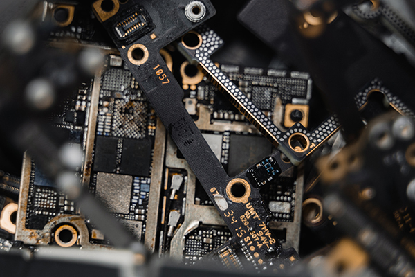
The component is fixed on the PCB by soldering through the lead hole on the PCB, then the lead hole and the surrounding copper foil are called pads. It is essential to have a rich knowledge reserve of pads for an excellent PCB engineer. Many people can draw pads according to the component manual, but it is not easy to draw good pads. AiXun shares some tips below, hoping to help you learn more pad basic knowledge.
Types of Pads
In general, the pads can be divided into 6 categories, which are distinguished according to the shape as follows:
1. Square pads - used when the components on the printed board are large and few, and the printed wires are simple. When making a PCB by hand, it is easy to use this pad.
2. Circular pads - widely used in single and double-sided printed boards with regular arrangement of components. If the density of the board allows, the pad can be larger so that it will not fall off during soldering.
3. Island-shaped pads - the connection between the pads and the pads is integrated. Commonly used in vertical irregular arrangement installation. For example, this pad is often used in tape recorders.
4. Teardrop pads - often used when the traces connected to the pads are thin to prevent the pads from peeling and the traces from being disconnected from the pads. This pad is commonly used in high frequency circuits.
5. Polygonal pads - used to distinguish pads with similar outer diameters but different apertures, which is convenient for processing and assembly.
6. Oval pad - this pad has enough area to enhance the anti-stripping ability, and is often used in dual in-line devices.
7. Open-shaped pads - commonly used to ensure that the pad holes of manual repair soldering are not sealed by solder after wave soldering.
Dimensional Standards for Pads in PCB Design
1. The minimum single side of all pads is not less than 0.25mm, and the diameter of the entire pad is not greater than 3 times the aperture of the component.
2. Try to ensure that the distance between the edges of the two pads is greater than 0.4mm.
3. In the case of dense wiring, it is recommended to use oval and oblong lands. The diameter or minimum width of the single-sided pad is 1.6mm; the double-sided weak current circuit pad only needs to add 0.5mm to the hole diameter. If the pad is too large, it will easily cause unnecessary continuous soldering. The hole diameter exceeds 1.2mm or the pad diameter Pads exceeding 3.0mm should be designed as rhombus or quincunx pads.
4. For plug-in components, in order to avoid copper foil breakage during soldering, the connection pads on one side should be completely covered with copper foil; the minimum requirement for double-sided boards should be filled with teardrops.
5. All machine plug-in parts must be designed as drip pads along the direction of the bend to ensure that the solder joints at the bend are full.
6. The pads on the large-area copper skin should use chrysanthemum-shaped pads to prevent false soldering. If there is a large area of ground wire and power wire area (more than 500 square millimeters) on the PCB, a window should be partially opened or designed as a grid filling.
Some requirements for pads in PCB manufacturing process
1. If the two ends of the SMD component are not connected to the plug-in component, a test point must be added. The diameter of the test point is preferably between 1.0mm and 1.5mm, so as to facilitate the test of the online tester. The edge of the test point pad should be at least 0.4mm away from the edge of the surrounding pads. The diameter of the test pad must be more than 1mm, and must have network attributes. The center distance between the two test pads should be greater than or equal to 2.54mm; Above 1mm (inclusive);
2. Pads must be added where the holes with electrical connections are located; all pads must have network attributes. For networks without connected components, the network names cannot be the same; the distance between the center of the positioning hole and the center of the test pad is more than 3mm; other irregular shapes, but with electrical connection slots, pads, etc., are uniformly placed on the mechanical layer 1 (referring to single Slotted holes such as inserts, fuses, etc.).
3. Component foot pads with dense pin spacing (pin spacing less than 2.0mm) (such as: IC, swing socket, etc.) must be added to the test pad if they are not connected to the hand plug-in pad. The diameter of the test point is preferably between 1.2mm~1.5mm, so as to facilitate the test of the online tester.
4. If the pad spacing is less than 0.4mm, white oil must be spread to reduce continuous soldering during wave peaks.
5. The two ends and ends of the SMT components in the dispensing process should be designed with lead tin. The width of lead tin is recommended to use 0.5mm wire, and the length is generally 2mm or 3mm.
6. If there are hand-soldered components on the single panel, the tin bath should be removed, the direction is opposite to the direction of passing the tin, and the size of the width viewing hole is 0.3mm to 0.8mm;
The above information comes from the Internet. If you have any questions, feel free to contact AiXun Smart Precision Soldering Experts.
 WhatsApp