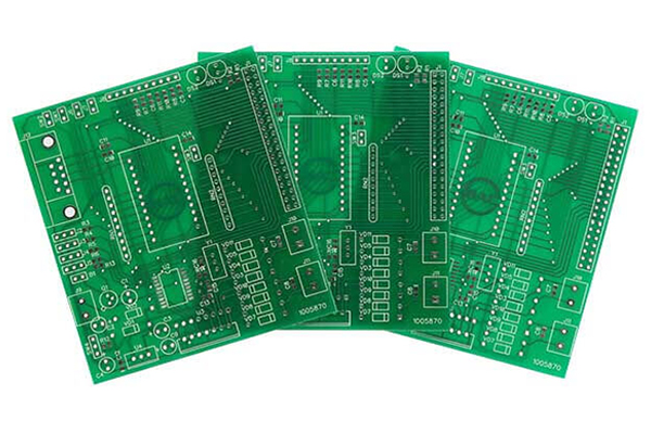
Today, Aixun Precision Soldering will review the history of PCB with you.

Review the history of PCB printed circuit board development in the early 20th century: the first batch of printed circuit board patents "printed wires" were issued in the early 20th century, but the industry-recognized PCB printed circuit board was first put into use after World War II. In 1925, American Charles Ducas filed a patent application for a method of forming electrical paths directly on insulating surfaces by stencil printing with conductive ink. Austrian scientist Dr. Paul Eisler invented the first operational printed circuit board in 1943.
1920s
The earliest printed circuit boards (PCBs) were made from materials such as Bakelite, wood-based panels, layered cardboard, and even thin wood. Holes are drilled into the material, and flat brass "wires" are riveted or bolted to the board. The connection to the component is usually made by pressing the end of the brass trace onto the pop rivet, while the lead from the component is simply pressed into the open end of the rivet. Occasionally small nuts and bolts are used instead of rivets. This form of circuit board was used in early tube radios and phonograph products.
1950s~1960s
Laminates made using different types of resins and material mixes were introduced, but PCBs were still single-sided. Board and components are on different sides. Compared with bulky wiring and cables, the advantages of PCB make it the first choice for new products to enter the market. But the biggest influence on the development of printed wiring boards came from the government agencies responsible for developing new weapons and communications equipment, which used end-of-line assemblies in some applications. After the leads of the components were placed through the holes, small nickel plates on the leads were held in place by soldering on the board.
Late 1960s
The production process of printed circuit boards evolved dramatically, culminating in the development of a process for plating copper onto the walls of drilled holes. This allows the circuits on either side of the board to be electrically connected. Copper has replaced brass as the metal of choice because of its ability to carry electrical current, and its relatively low cost and ease of fabrication. In 1956, the U.S. Patent Office issued a patent for a "process of assembling electrical circuits," which was applied for by a small group of scientists represented by the U.S. Army. The patented process involves using a substrate, such as melamine, to laminate copper foil and trace the circuit pattern, which is then photographed, much like an offset printing plate. The acid-resistant ink side printed on the copper foil board is etched to remove the exposed copper, leaving "printed lines". Then, use the die to punch holes in the graphic to match the location of the component wires or terminals. The leads are passed through the non-plated holes in the laminate, and the card is dipped or floated on a bath of molten solder. Solder covers the bead and connects the component's leads to the bead. This is the prototype of the current PCB printed circuit board process.
1980s to present
PCB printed circuit board technology has developed rapidly, evolving from early single-layer boards to multi-layer boards, and advancing from 6mil line width and line spacing to 3mil. It is gradually able to produce circuit boards with extremely high precision and high frequency requirements, such as HDI, blind buried vias and other processes. And the development of the entire printed circuit board industry is also highly automated. The introduction of various precision exposure machines, etching, and electroplating equipment makes PCB more miniaturized and miniaturized, thereby meeting the requirements of the current era of electronic products.
The development history of PCB is also the history of semiconductors. At present, the 5nm process technology is coming soon, which means that we can condense more complex products onto smaller PCB. Since 1925, the development of PCB has become mature, and the industry's process technology is relatively perfect. Even the production of FPC flexible printed circuit board and rigid-flex printed circuit board is becoming more and more proficient. The history of PCB is a history of technological transition, which has witnessed the efforts of countless people in this industry.
>> Click AiXun soldering tools to know more basic knowledge of PCB
 WhatsApp