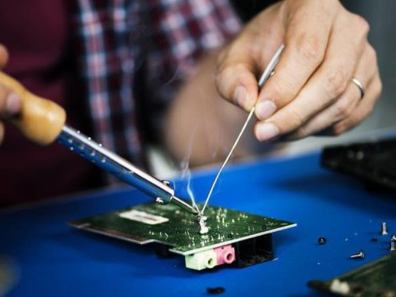
With the development of electronic products, circuit boards are becoming more and more light, thin and small, and PCBs are also developing in the direction of high quality, high density and high difficulty, and customer requirements are getting higher and higher. The requirements for holes are also getting higher and higher.

For example, there must be no solder mask ink entering the holes, causing solder balls to hide in the holes, no frying, difficult to mount components, etc.
Application of PCB over-hole plug: Prevent tin from passing through the component surface from the via hole to cause short circuit during PCB wave soldering, avoid flux residue in the via hole, prevent the solder ball from popping out during wave soldering, causing short circuit, and prevent the surface solder paste from flowing into the hole. False soldering affects mounting, maintains surface flatness, and meets customer characteristic impedance requirements.
PCB plug hole requirements: the via hole is covered with copper, and the solder mask can be plugged or not; the via hole must have tin and lead, and must have a certain thickness requirement (4um), no solder mask ink enters the hole, causing hidden holes in the hole Solder beads; through holes must have solder resist ink plug holes, opaque, and must not have tin circles, tin beads, and leveling.
 WhatsApp